DDA and FDTD Modeling of Optical Properties of Silver Metal Nanoparticle Assembly Obtained by Thermal Evaporation and Annealing On Sno2 Glass Substrate for Implementation in Thin Film Solar Cells
We used silver metal nano particles in order to improve the poor efficiency of second generation hydrogenated amorphous silicon solar cells. Such Metal nano particles are known to generate strong localized surface plasmon resonances at ultraviolet, visible and near infrared wavelengths which might improve the light absorption and then the efficiency of the cell
We reported previously an improvement of about 14 – 15% of the spectral response by implementing silver nano particles of 70nm mean diameter on the rear face of the cell.
Finite difference time domain and discrete dipole approximation modeling have been carried out to explain the decay of the surface plasmon resonance to the higher wavelengths and the appearance of several resonance modes correlated with the increase of the spectral response.
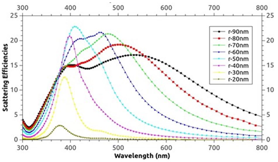
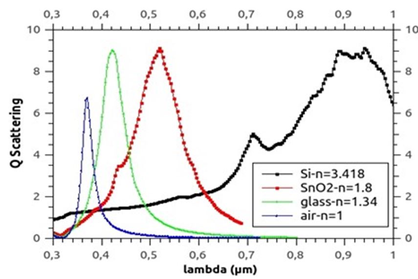
Finite difference time domain model have been used for an isolated spherical particle. By increasing both the particle size and medium refractive we have exhibited the decay of the surface plasmon resonance to the red part of the spectra and the appearance of several modes.
Discrete dipole approximation model was performed on an assembly of nano particles taking into account the real shape of the particles from experimental data leading to a decay of the scattering efficiency towards red and infrared part of the spectra with the increase of particles mean diameter and the coupling effect, that is in strong correlation with our experimental results.
Keywords:Plasmon; Photovoltaic; Nanoparticles; Silver; Discrete Dipole Approximation; Finite Difference Time Domain Modeling
While interacting with the incident light, the NP conduction electrons exhibit their sole optical properties: The collective oscillations of the free electrons at the surface of a conductor which are known as surface plasmons [1]. In the case of nanostructures, localized surface plasmon resonances (LSPRs) induces a high local field In response to light exposure at optical frequencies, metal NPs exhibit efficient light extinction as a consequence of the LSPRs excitation. This extinction has been found to be NP composition size, shape, and dielectric environment dependent. [2] The pioneering work of Gustav Mie [2] on metal nanoparticles leaded up to their use in various research areas, making them of immense technological importance [2].
The theoretical and numerical tools on complex LSPR spectra are reported in the literature. [2] Mie theory and related methods provide a full analytical solution for a symetric particle (sphere, cylinder, spheroid) under an incident plane wave [2]. Here LSPRs then appear as a specific type of plasmon-induced resonances of the extinction cross sections. Extinction spectra describes the nanoparticle’s ability to perturb incident light, either by scattering or absorption. Non-spherical metal NPs have optical properties that strongly depend on their shape complexity as seen from the analytical solutions derived for simple geometries mentioned above. For more complicated geometries, however, the theoretical formalism appears to be more complicated and Mie theory reaches its limits.. Numerical simulations have therefore to be employed when considering the scattering from NPs with arbitrary sizes and shapes which may interact. Reliable numerical methods allow the investigation study of scattering (and related) problems in the Classical Electrodynamics paradigm [1].
The classical electro dynamical models usually employed to study the optical properties of metal NPs based devices rely on the local dielectric function ε(ω) as their only material-related parameter. Therefore, the results obtained from these models can only be as accurate as the permittivities of the NP material and the embedding medium. Some of the most used datasets for silver are the ones from Palik and the ones from Johnson and Christie. [2] They can both give quite different results. One dataset could give much higher field enhancement at the resonance wavelength compared to another. Since ε is a macroscopic material property, one finds classical electrodynamical approaches with phenomenological corrections and quantum models in order to account for size and non-local effects [4-10]. We can mention very recent references relative to re-evaluations of the optical constants of a few metals [3].
Simulated spectra are usually calculated for mono-sized and mono-shaped periodic arrays of particles. Discrepancies between measured and simulated curves come from the differences between the simulation tool and samples in which NPs display random size and shape distribution ensembles. To account for the size differences, weighted average spectra have been calculated from the experimentally determined size- distribution, suggesting that the measured spectrum can be considered as a superposition of spectra from various particles size. [3] A good qualitative agreement between experimental measurements and simulations was found, although the average spectrum neglected some experimental parameters, such as the irregular shape of NPs and the interaction among particles with different size. Moreover, the basic models employed often consider an isolated particle in a dielectric effective medium assuming homogenous in-plane properties. the stratified substrate can be take into account in these models by using simple analytic methods such as a definition of an average or effective refractive index. [6] There is a need for more elaborated models which rely on realistic characterization by microscopy and include multi-layered substrate systems whose effects are too important to neglect. In this work, we use the Finite Difference in the Time Domain (FDTD) and the Discrete Dipole Approximation (DDA) to find the LSPRs of sets of silver nanoparticles in configurations related to the experimental one. The influence of the physical environment on the LSPRs is studied. By environment, we do not only mean a single nanoparticle in a surrounding medium with dielectric constant > 1, but also the presence of substrates, and other close enough silver nanoparticles with different sizes and shapes.
Both numerical methods are used in a complementary manner, and are suitable for nanoparticle of arbitrary shapes. FDTD is used to model the influence of the substrates while DDA is used to account for the LSP modes coupling from several particles.
SEM pictures of silver nano particles assembly, obtained by thermal evaporation of a 6 nm layer of silver and annealing, are used as case study for the validation of the models. The SEM pictures give access to the distribution size and shape of the nano particles assembly. We consequently show that the nano particles lead to an improvement of the scattering in the red and infrared part of the spectra.
We investigated if PA-IGT was able to detect differences between our four samples: Athletes, Non-Athletes, Anorexia Nervosa patients with Excessive Physical Activity (AN-EPA) and Anorexia Nervosa patients without Excessive Physical Activity (ANWEPA). Based on IGT results, we expected Athletes and Non-Athletes not to differ in their performances and the patients! groups to obtain worse performances, without significant differences between AN-EPA and AN-WEPA. Concerning PA-IGT, we expected Athletes to perform better than Non-Athletes and better than AN patients (i.e. AN-EPA and AN-WEPA). Between the patients’ groups (i.e. AN-EPA and AN-WEPA), we expect AN-EPA to obtain the worse score. A similar study maintained the tripartition of the experimental sample in healthy athletes, healthy non-athletes and AN patients [30], while we further divided our sample into AN with and without EPA. As a result, we expected AN-EPA to show a worse performance than AN-WEPA, being the EPA symptom specific of this sample.
The finite-difference in time-domain (FDTD) is a time method based on the discretization of Maxwell's equations on a mesh formed of rectangular parallelepipedic cells. It is one of the widely used method for the calculation of the optical properties of nanostructures [6-8].
The formalism is very simple and allows, from a single short pulse in the time-domain, the study of the full spectrum on a wide band, using a discrete Fourier transform. In the standard approach, the temporal and spatial derivatives are approximated by second-order central finite differences in order to determine the evolution of the three dimensional electric and magnetic fields components in each cell. Half-steps are used to discretize time and space within a special time update algorithm due to Yee, [22] and calculations on both the spatial and temporal domains are nested. More specifically, the electric field is calculated for half-time steps and whole steps of space, while the magnetic field is calculated for whole steps of time and half-steps of space. The derivation of the relevant expressions have been documented extensively in the literature and will not be repeated here. The FDTD is able to model light propagation, scattering, absorption, diffraction, reflection, and polarization effects. The description of metal nanoparticles and the surrounding or embedding insulating media is performed via analytical patterns of the frequency dependent dielectric functions of the different target materials placed in the computational cell. These functions are further Fourier transformed into the time-domain.
By choosing realistic computational parameters close to the experimental values, it is possible to compare simulated and measured results. The accuracy of the model is checked via preliminary tests with relevant reference structures. Then extinction spectra of the ensemble are calculated as functions of various parameters as particle size, particle shape, particle position in the device, thicknesses of the substrate and active layers within the sample. For the semiconducting layers, different fitted models are used for the dielectric function. The optimization of the optical properties of the sample can be achieved by direct comparison between simulated and experimental results.
The model of the solar cell structure is drawn based on SEM images of the real sample. We use a FDTD implementation (MEEP) [22] that allows designs ranging from simple to more complex geometries and include a wide variety of material. Drude–Lorentz dispersion model is used to model metal nanoparticles and semiconductor structures. In fact, the bulk experimental values of ε(ω) are modeled to fit a rational polynomial with mutiple terms refering to Debye, Drude or Lorentz approximations. The Drude term provides a satisfactory description of the dielectric permittivity of many free-electron-like metals in the near infrared part of the spectrum and accounts for the intraband behavior. The Drude model depends on two parameters only and remains accurate with experimental values while interband transitions are negligible, that is till 3.8 eV for Ag. To account for interband transitions, one or more Lorentzian oscillators are used. A large number of lorentzians provides a high quality fit but, by doing so, the model looses any physical meaning.
Typical initial conditions are plane-wave sources with gaussian pulses, as they produce a slow transition between high and low values and are capable of containing a broad range of frequencies. The propagation direction is y and the polarization direction is either x or z. The resolution is set to values between 1.7 and 3 nm. There is a need in the FDTD method of absorbing conditions around the discretized mesh. Perfectly Matched Layers [24 (PML), which are absorbing layers placed around the numerical domain to remove efficiently the influence of back-scattering fields are used. Monitor boxes are used to obtain the scattered power by the target. The power flowing outward through the faces of the monitor boxes is substracted out the power of the incident source to get the scattered power by the target. The scattering cross- section and efficiency are then deduced from the spectral intensity of the incident wave and the geometric projective area of the target. The accuracy of FDTD calculations is increased by using subpixel smoothing of the dielectric function and errors due to the discretization of discontinuous dielectric materials are thus minimized.
The discrete-dipole approximation is a numerical technique for calculating scattering and absorption of electromagnetic radiation by targets with sizes smaller than or comparable to the incident wavelength. In DDA, the structure of interest is approximated by a cubic array of N polarizable points (dipoles), notwithstanding its complexity or its shape. Polarizabilities are assigned at the dipole locations based on the physical properties of the target. The polarization at each location is then solved self-consistently in the presence of an incident radiation field. The results accuracy increases with the number of dipoles used to model the target. In order to get a good accuracy (error about 10% or less), a threshold of 10^4 dipoles is usually required. This number cannot be extremely large because of the computational costs induced. An important part of the method is the use of the appropriate expression for assigning dipole polarizabilities. In order to minimize the errors, the interdipole distance should be small compared to the dictinctive structural features of the target.
We use DDSCAT, a free code developed by Draine and Flatau [25, 26]. The value of N used in this work ranges between 3x10^4 and 10^6, depending on the complexity of the target. We employ the bulk dielectric function for silver measured by Johnson and Christy. Experimental procedure: Deposition and characterization of NPs
For elaboration of nano particles [1], we deposit by vacuum evaporation at ambient temperature a silver layer of 6nm on a SnO2 glass substrate, this technology is really low cost and one of the most employed in the field of amorphous silicon. The roughness of the substrate is about 6 ± 1 nm.
Typically, after deposition substrates are subsequently annealed at 300°C during 1 hour. This steps leads to the growth of the NPS The surface morphology of NPs was observed with a Hitachi S4500 FEG Scanning electron microscope (SEM) with an accelerating voltage of 5 kV.
Estimation of shape and size distribution of silver Nano Particle through SEM observations
Figure 1 shows SEM pictures and associated size distribution of Ag NPs Compared
to virgin substrates (Figure 1a), growth of spherical Nano particles is evidenced after the thermal process, (Figure 1b). The NPs diameter ranges are estimated through Image J software and are estimated to be between 20 to 130 nm with a mean diameter of (75± 20) nm (see Figure 1c).
From these SEM observations and estimation of nanoparticles size several calculations have been lead. First FDTD model have been used to determine the influence of the particle size and medium refractive index for a spherical isolated nano particle. In a second way DDA model give access to the scattering spectra of first two nanoparticles with various distances, and secondly for an assembly of nano particles extract from the SEM pictures.
For an isolated particle the increase of particle size from 20 to 90nm or refractive index from n=1(air value) to n= 3.418(Si value) systematically lead to a decay of the SPR in the infrared part and the appearance of several resonance modes. Increasing the particle size from 20 to 90nm lead to a decay of the first mode from 380nm to 540nm and the appearance of a second mode. Increasing the refractive index from n=1 to n=3.418 lead to a decay from 350 to 900nm.
First simulations were achieved to determine the coupling effect of two identical particles (60nm in diameter) in air. The linear polarization of the electric field is orientated along the Z axis.
Axis passing through the center of the Nano particles is parallel to the y axis and x is the light propagation direction. g is the distance between two Nano particles
We point out (Figure 4) that when the distance between the two nanoparticles is lower than the mean diameter there is a decay towards the higher wavelengths and the appearance of several resonance, this phenomenon is of real interest for the lack of absorption of solar cells in the infrared part of the spectra.
For an assembly of nanoparticles two areas have been chosen from the SEM pictures, respectively identified as zone 1(Figure 5) and zone 2(Figure 6). Particles have been considered to be spherical and size have been estimated from the SEM pictures. For DDA simulations several particles mean diameters have been considered and to be in direct contact with the smooth SnO2 substrate The results consequently point out the appearance of several plasmon resonance modes with a systematic decay in the infrared part of the spectra as the particles size are increasing.
In order to match as well as possible, the SEM results we have taken into account the real shape of the particles (Figure 7) in air or in SnO2 as a surrounding medium
Consequently, for the two index values (n=1 in air and n=1.8 in SnO2) we point out a decay from 400 to 600nm for 50nm particles size and from 450nm to 700nm for particles of 75nm and a broadening of the scattering curve.
These results are in good correlation with our previous observation [28] on the effect of Ag NPs on the efficiency of amorphous industrial cells build by SOLEMS Company [29]
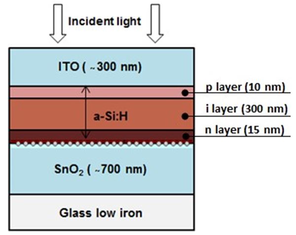
As shown in Figure 8 AgNPs were placed on the back side of the cell. The substrate is a glass one with a SnO2 700nm coating
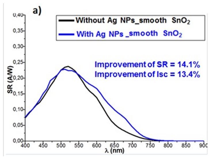
Typical spectral response shown in Figure 9 has evidenced an increase of the SR and Isc of the cells with NPs respectively about 14% and 13.4%.
Silver nano particles were obtained after deposition [1] of a 6nm layer of silver on a smooth SnO2 substrate. and a subsequent annealing at 300°C. SEM observations of the silver nano particles give access to their size distribution and shape, which are considered to be spherical with a mean diameter around 70 nm.
FDTD modeling clearly exhibit the decay of the scattering efficiency towards the higher wavelength as the particle size and medium refractive index increase and the appearance of several resonance modes especially interesting for improving the spectral response of thin film solar cells.
DDA model achieved on two nanoparticles to exhibit the coupling effect was secondly used on an assembly of nanoparticles exhibiting a decay of the scattering efficiency towards red and infrared part of the spectra with the increase of particles mean diameter and the coupling effect, which is in strong correlation with our previous experimental results. Real shape of the Nano particles have also been implemented in order to match as well to the experimental results The deposition method clearly lead to particle size in the interesting range (Around 100nm) which lead, associated with coupling effects, to a decay of the scattering towards the infrared part of the spectra especially interesting for improving solar cells efficiency.
// DDSCAT: http://ddscat.wikidot.com/
We would like to acknowledge the Centre for High Performance Computing in Cape Town and the Centre for Intensive Computing (C3I) in the University of the West Indies and their staff for the access to the computational facilities.

.JPG)
.JPG)
.JPG)


.JPG)
.JPG)
.JPG)
.JPG)
.JPG)
.JPG)
.JPG)
.JPG)
.JPG)
.JPG)
.JPG)
.JPG)

