Diffuse Reflectance Spectra for Sulvanites Cu3TaVI4 (VI: S, Se and Te)
Polycrystalline samples of Cu3TaVI4 (VI: S, Se and Te) were prepared by the melt and anneal method. X-Ray Diffraction (XRD) and Diffuse Reflectance Spectroscopy (DRS) measurements were performed in order to verify the crystal structure and calculate the indirect and direct band gaps of the obtained samples. Their respective absorbance spectra were compared with the optical absorption coefficient obtained by means of first-principles calculations.
Keywords: Sulvanites; Diffuse Reflectance; Optics; Optical Band Gap
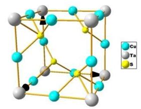
Sulvanite-type compounds Cu3-MT-VI4 (MT= V, Nb or Ta; VI= S, Se or Te) have generated a lot of interest because of their behavior as transparent p-type semiconductors with high mobility, making them good candidates for transparent electronics [1-4] and also as good photovoltaic materials because of their indirect gap of approximately 1.5 eV [5]. These compounds crystallize in the cubic P43m (215) structure consisting of Cu, MT and VI atoms which are positioned at: 3d (0.5, 0, 0), 1a (0, 0, 0) and 4e (u, u, u) Wyckoff positions, respectively [6-8] (Figure 1). A summary of the structural parameters was given in a previous report [9].
Optical energy gaps of Cu3TaS4 and Cu3TaSe4 have been measured and calculated previously; and also, optical absorption coefficients have been calculated in the energy range up to 20 eV for Cu3-MT-VI4 (MT: V, Nb, Ta; VI: S and Se) compounds [3,9-11]. Diffuse reflectance is a well-known technique that provides important information about the absorption bands of materials and it was frequently used in mineralogy [12-15]; moreover, it provides an experimental tool to verify first-principle calculations of the optical properties of semiconductors as it is the case of the optical absorption coefficient. In this work we report measurements of optical absorbance of Cu3TaVI4 (VI. S, Se, Te) compounds in the energy range 0.5 to 6 eV and the obtained experimental spectra are compared with those previously calculated and reported in literature.
Polycrystalline ingots, of about 1 g were prepared by the usual melt and anneal technique. Starting materials with a nominal purity of 99.99 wt. % in the stoichiometric ratio were mixed together in an evacuated (10-4 Torr) and sealed quartz tube with the inner walls previously carbonized in order to prevent chemical reaction of the elements with quartz. The quartz ampoule was heated up to the melting point of the anion (S, Se or Te) kept at this temperature for 48 h and continuously shaken by means of an electromechanical motor. This procedure guarantees the formation of binary species at low temperature, avoiding the existence of anion vapor at high temperature, which could produce explosions or anion deficiency in the product ingot. Then the temperature was slowly increased until 1423 K, with the mechanical shaker connected for a better mix of the components. After 24 h, the cooling cycle began until the anneal temperature (800K) with the mechanical shaker disconnected. The ampoule was kept at the annealing temperature for 1 month in order to assure that thermal equilibrium was reached. Then the furnace was switched off.
X-ray powder diffraction data were collected by means of a diffractometer (Bruker D5005) equipped with a graphite monochromator (CuKα, λ = 1.54059 Å) and an X-ray tube power of 40 kV and 20 mA. Silicon powder was used as an external standard. The samples were scanned from 10–100º 2θ, with a step size of 0.02° and counting time of 20 s/step. The Bruker analytical software was used to establish the positions of the peaks and the CuKα2 components was removed from the data using a mathematical function. The peak positions were extracted by means of single-peak profile fitting carried out through the Bruker DIFFRACplus software. Each reflection was modeled by means of a pseudo-Voigt function.
Optical absorbance has been measured in the energy range 0.5 to 6 eV using Diffuse Reflectance Spectroscopy (DRS) technique using a UV-Visible-IR spectrophotometer equipped with a diffuse reflectance accessory (integrating sphere) capable of collecting the reflected flux. The sample was grinding in an agate mortar in order to obtain a fine powder (<10μm). Barium sulfate (Merck DIN 5033) was used as internal standard.
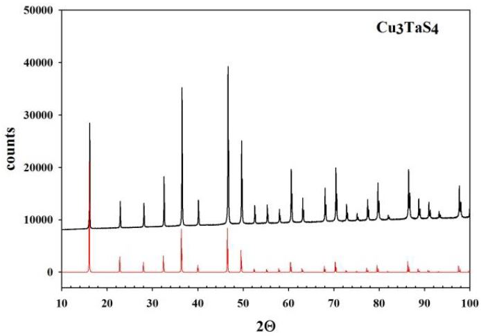
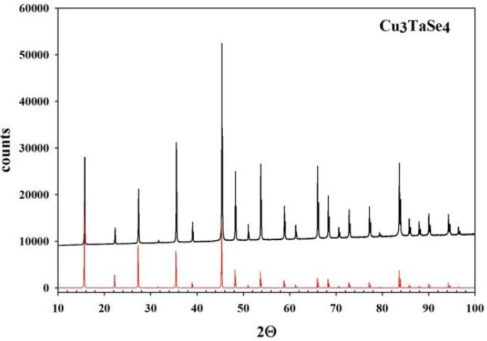
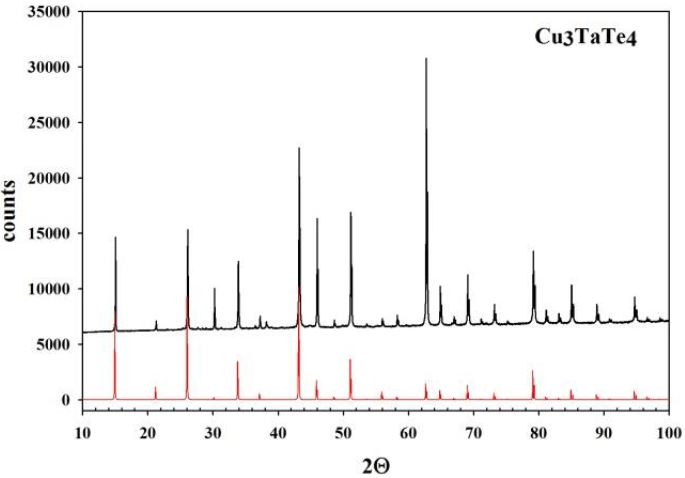
In Figure 1,Figure 2 and Figure 3, the experimental diffraction patterns for Cu3TaS4, Cu3TaSe4 and Cu3TaTe4 are displayed.
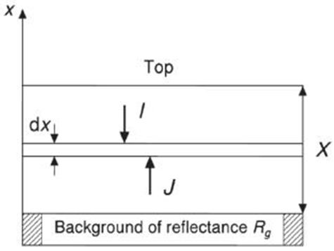
No extra lines due to secondary phases are observed in the diffraction patterns indicating that the samples correspond well to Cu3TaS4, Cu3TaSe4 and Cu3TaTe4; however, differences in the experimental peak intensities with respect to calculated suggests some disorder in the samples due to their polycrystalline character and also possibly some preferential orientation in the powder particles. The Kubelka-Munk theory assumes that a plane-parallel layer of thickness X capable of both scattering and absorbing radiation is irradiated in the –x direction with a diffuse monochromatic radiation flux I (Figure 4) [17,18]. The layer is very extensive relative to x and can be split into infinitesimal layers of thickness dx. The diffuse radiation flux in the negative and positive x directions are designated I and J, respectively. If, in the passing through dx the downward flux I is decreased by an amount KIdx by absorption, and increased by an amount SIdx by scattering, and a similar reasoning is made for the upward flux J, then the following differential equations can be derived:
Where K and S are the absorption and scattering coefficient of the sample, respectively
The explicit hyperbolic solutions to this equations obtained by Kubelka were discussed in detail by Wyszecki and Stiles [19].
The most general solution is:
Where R is the reflectance of the layer over a background of reflectance Rg, X the layer thickness, a = 1 + K/S and b = (a2-1)0.5.
Generally, measurements are made on layers thick enough to ensure that a further increase in thickness will fail to change the reflectance. Under these conditions, the reflectance is given by R∞ and Equation 3 yields:
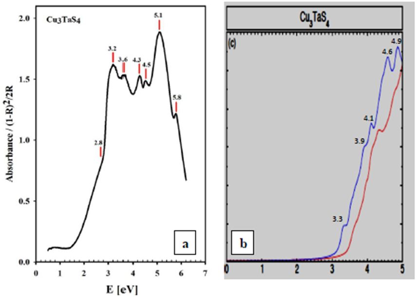
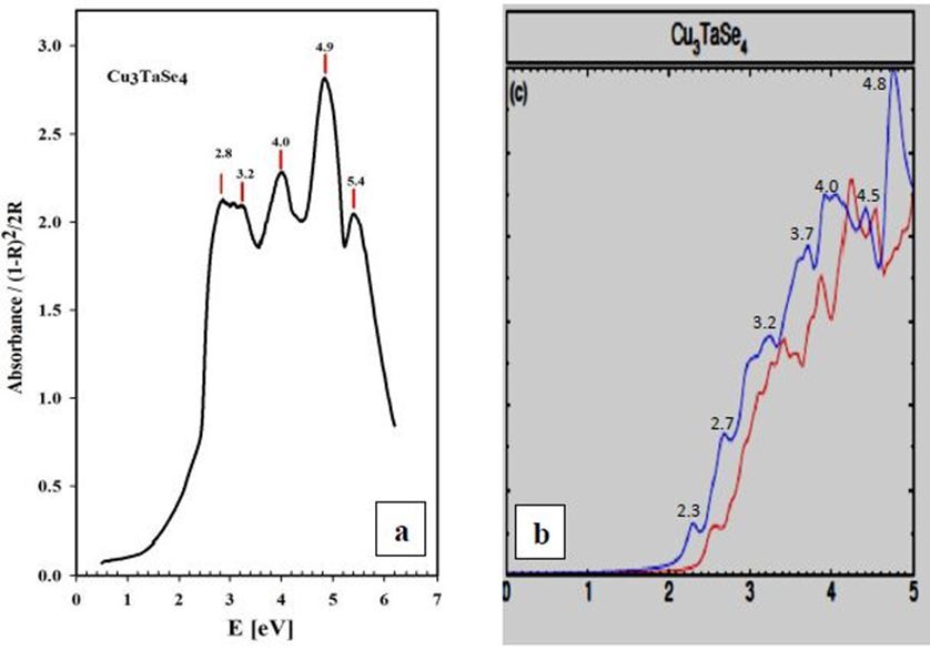
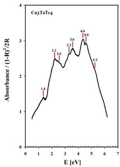
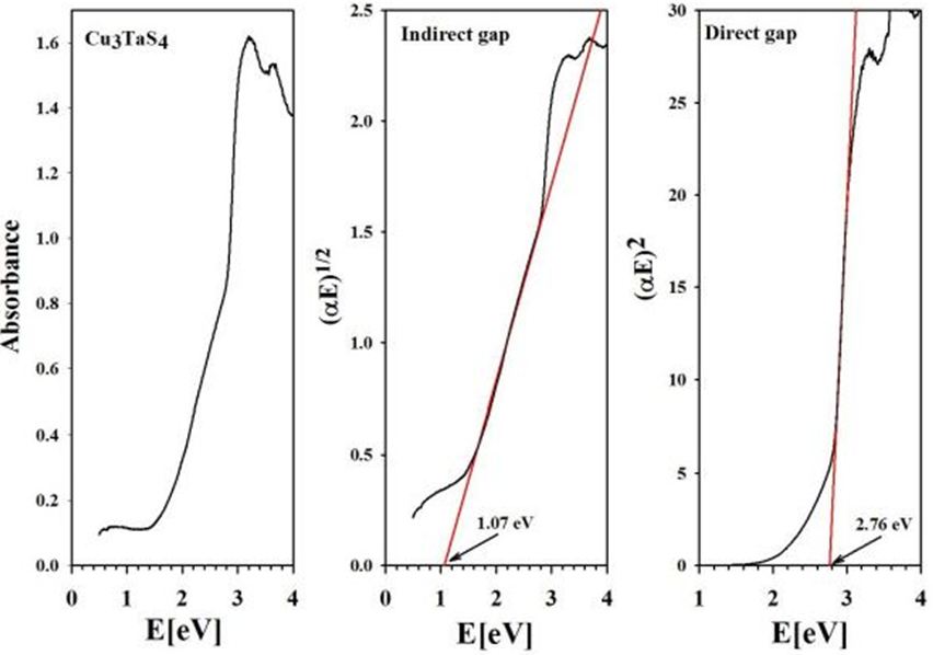
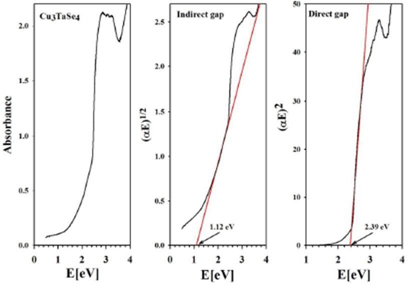
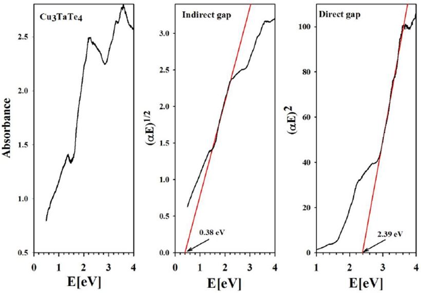
Where F(R∞) is usually termed the remission or Kubelka-Munk (K-M) function. In Figure 5,Figure 6 and Figure 7, the K-M function for Cu3TaS4, Cu3TaSe4 and Cu3TaTe4 are given.
Experiment and theoretical calculations coincide very well especially for the BSE method. Both compounds are transparent for energies lower than 2 eV as it is expected for the color of the samples (light yellow); the absorption increases from 2 eV until 5 eV, and then decreases. The relative maxima at 5.1 eV (Cu3TaS4) and 4.9 eV (Cu3TaSe4) observed in the experiment match very well with the calculated maxima for the optical absorption coefficients, 4.9 eV (Cu3TaS4) and 4.8 eV (Cu3TaSe4). In Table 1, the observed and calculated maxima for the absorption bands, for both compounds are show for comparison.
From the absorbance spectra, the direct and indirect energy gaps of Cu3TaS4, Cu3TaSe4 and Cu3TaTe4 were obtained (Figure 8,Figure 9 and Figure 10)
From our measurements, Cu3TaTe4 shows a direct optical band gap at the -point of 2.39 eV in good agreement with the calculated value of 2.57 eV [17,18]. For Cu3TaS4 a direct optical transition between the highest valence band and the lowest conduction band at the -point has been calculated at 3.36 eV, 3.6 eV and 1.91 whereas an experimental report previous to this work gives a value of 2.70 eV that coincides with the value measured in this work of 2.76 eV; it seems that theoretical values over- or sub-estimated according to the procedure [10,11,15]. For Cu3TaSe4, all the experimental values 2.35 eV 2.43 eV, including this work 2.39 eV, agrees very well; and also, the calculated 2.57 eV is very close to experimental [3,9,17,18]. The obtained experimental absorbance spectra of Cu3TaS4, Cu3TaSe4 and Cu3TaTe4 show that these compounds absorb radiation in a wide range of energy, from 1 to 6 eV. In the case of Cu3TaS4 and Cu3TaSe4 they absorb strongly in the 3 to 5 eV which makes these compounds suitable as optical detectors in the visible and near ultraviolet range. For Cu3TaTe4, the maximum absorption is in the range 2 to 5 eV, wider that Cu3TaS4 and Cu3TaSe4, in consequence this material can be used as an optical detector from the near infrared to the near ultraviolet range. From the point of view of photovoltaic applications, these compounds can be used as absorbers, since they are p-type and have indirect gaps in the near infrared (infrared in the case of Cu3TaTe4) and direct gap in the visible part of the solar spectrum. Additionally, Cu3TaS4, Cu3TaSe4 are transparent materials (the only transparent Cu-based compounds that are also p-type) which suggest the possibility of transparent solar cells with a wide range of photon absorption [21,22].
Optical absorbance measurements were performed on Cu3TaVI4 sulvanites (VI. S, Se, Te) in the energy range 0.5 to 6 eV. The obtained spectra were compared with previous calculations by first principles and the agreement is very good. From the absorbance curves the direct and indirect optical band gaps were obtained using Tauc’s plots and compared with previous reports. It was found that direct transition values agree very well with experimental and theoretical reports with the exception of Cu3TaS4 for which the theoretical values seems to be over- or sub-estimated.

