
Laser Synthesis of Variable Band Gap 2D Structures for High Sensitivity Thermo-Photo Sensors Received in the Reaction of Chromium Atoms with Methane Molecules
Semiconductor materials with variable band gap are of great promising materials as they are more effective materials as photovoltaic converters and sensors in comparison with single band gap materials. Photons of a KrF laser (248 nm) were used for the synthesis of variable band gap 2Dstructures in the reaction of Cr atoms with CH4 molecules by reactive pulsed laser deposition (RPLD). 2D structures were deposited on 293 or 800 K <100> Si substrate at CH4 pressure of 1.0 or 3.0 Pa resulted in changing of their structures’ thickness in the range of (30-90) nm. These deposits reveal amorphous or polycrystalline structure. Element analysis was carried out by an energy dispersive X-ray spectroscopy (EDXS). All synthesized 2D structures demonstrated semiconductor temperature trend with variable energy band gap (Eg) in the range of (0.45-2.1)eV depending on substrate temperature, CH4 pressure in the reactor and 2D structure thickness. Optimum experimental parameters were found out to obtain the highest photosensitivity of this 2D structure. The highest obtained photosensitivity was about 700 VC/W at white light power density ~ 6x10⁻³ W/cm2. VC is “chemical” photo electromotive force induced in the deposited 2D structure while irradiating it with white light, W is white light power. The highest obtained thermo-sensitivity (Seebeck coefficient, S) was about 2.6 mV/K. Photo sensitivity and thermo-sensitivity nature of the synthesized 2D structure in these conditions was explained. Therefore, such 2Dstructuresexhibiting high photosensitivity and high thermo-sensitivity are exceptionally strong candidates for effective photo-thermo sensors operating at moderate temperature
Keywords:Laser Synthesis; Semiconductor; Thermo-Photo Sensor
At present, great interest is growing up for 2D structures to test the advantages of reduced thickness on the performances of electronic devices and sensors [1]. As it was shown in our previous works, 2D structures based on transitional metals’ silicides and oxides synthesized by pulsed laser deposition (PLD), reactive pulsed laser deposition (RPLD) and laser chemical vapour deposition (LCVD) are of great promising materials for thermo-tenso-photo-chemical sensors [2-8]. These silicides and oxides demonstrated semiconductor properties with energy band gap (Eg) less than 1.0 eV. RPLD was applied for the first time to synthesize of iron oxide 2D structures on<100> Si substrate for thermo-chemical sensors [3]. Also, RPLD was used for the synthesis of iron oxide 2D structures on Si substrate for thermo-photo-chemical sensors [7,8]. Nevertheless, there is a great problem dealt with white light spectrum energy conversion, i.e. sun’s spectrum conversion into electrical energy and, therefore, with high sensitivity of materials to white light as much as possible in. Semiconductor materials with variable band gap are of great promising materials as they are more effective materials as photovoltaic converters in comparison with single band gap materials. Before, semiconductor materials based on Cu(In,Ga)(Se,S)2 structure was synthesized with variable band gap from 1.04 to 1.7 eV for In/Ga and Se/S content in this structure [9,10]. As it is known, chromium oxide thin films (2D structures) with stoichiometry Cr3-xO3-y (0
Here, we used RPLD based on a KrF laser for the synthesis of the 2D structures with high S coefficient and high F. To decide this problem we used the reaction of ablated Cr atoms with CH4 molecules. These deposited structures on <100> Si substrates demonstrated semiconductor properties with variable band gap. The synthesis of the 2D structures was carried out at different experimental conditions to find out optimum ones to obtain as high as possible F and S parameters. Nature of high photosensitivity and thermo-sensitivity of these 2D structures was found out.
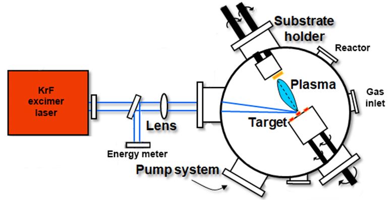
Each 2D structure was synthesized of ablated Cr atoms by KrF laser in the reaction with CH4. RPLD method gives the possibility to synthesize 2D structure with high purity at definite stoichiometry in direct process. 2D structure depositions were carried out in a stainless-steel vacuum reactor. Before each deposition, the reactor was evacuated down to a residual pressure of ~ 4.5x10⁻⁵ Pa to avoid contamination. Then, the flux of pure CH4 (99.999%) was introduced and stabilised to the desired dynamic pressure in the range of (1.0-3.0) Pa. A pure Cr (99.5%) targets were ablated with a KrF(λ = 248 nm) excimer laser pulses at a fluence of (4.0-4.5) J/cm2, a frequency repetition rate of 10 Hz and a laser pulse duration of 25 ns. Each 2D structure was deposited on high-resistance <100>Si substrate, i.e. substrate thickness is about 0.03 cm and specific conductivity of Si (σ  2x10⁻⁵ (Ωxcm)-1) by a definite number of laser pulses (N), which could be changed from 1000 to 9000 depending on each 2D structure’s thickness. The Cr target was rotated at a frequency of 3 Hz to avoid piercing and ensure a smooth ablation procedure. Before each deposition, the target surface was cleaned by 3000 laser pulses at a fluence of 4.5 J/cm2 with a shutter shielding the substrate. Substrates were parallel at 45-mm distance from Cr target and cleaned before in an ultrasonic bath with acetone, ethylic alcohol and finally rinsed in deionised water. Synthesized 2D structures at fluxes of ablated Cr atoms at definite methane pressure and definite number of laser pulses were deposited on room temperature (RT) or heated Si substrate. The principal scheme of the setup based on RPLD for the synthesis of the 2Dstructure is shown in Figure 1
.
2x10⁻⁵ (Ωxcm)-1) by a definite number of laser pulses (N), which could be changed from 1000 to 9000 depending on each 2D structure’s thickness. The Cr target was rotated at a frequency of 3 Hz to avoid piercing and ensure a smooth ablation procedure. Before each deposition, the target surface was cleaned by 3000 laser pulses at a fluence of 4.5 J/cm2 with a shutter shielding the substrate. Substrates were parallel at 45-mm distance from Cr target and cleaned before in an ultrasonic bath with acetone, ethylic alcohol and finally rinsed in deionised water. Synthesized 2D structures at fluxes of ablated Cr atoms at definite methane pressure and definite number of laser pulses were deposited on room temperature (RT) or heated Si substrate. The principal scheme of the setup based on RPLD for the synthesis of the 2Dstructure is shown in Figure 1
.
The morphology of the deposited structures was investigated with scanning electron microscopy (SEM) using Tescan Mira 3 LMU and their element analysis was investigated by energy dispersive X-ray spectroscopy (EDXS) using JSM-6490 LV JEOL equipment. The crystalline of the deposited 2D structures was studied by a Panalytical X’-Pert-Pro-triple-X-ray diffract meter with using Cu Kα1 radiation. The direct current (DC) electrical resistance of the deposited 2D structures was measured by two-probe technique. Ohmic contacts of 2D structures were made by silver paste coating or indium coatings Temperature dependences of the electrical resistance of the deposited 2D structures were measured with a high resistance multimeter. The calculation of the specific conductivity (σ) of the deposited 2D structure was performed taking into account these structures’ thickness (d) and the geometrical shape of Si substrate with the deposited structure (0.8x0.25) cm2. The thickness of deposited structures was measured by profile meter Alpha Step 200 “Tencor Instruments” with an error of 0.4 nm. Here, we synthesized the 2D structures on 293 or 800 K Si substrates in the reaction of Cr atoms with CH4 molecules at their pressure 1.0 or 3.0 Pa inside the reactor as optimum pressure for the highest value of the S coefficient and the photosensitivity F.
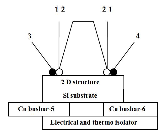
The S coefficient was studied in the range of (240-340) K. Special installation was used for temperature measurement of a sample and temperature difference (ΔT) between heated and room temperature (RT) end or cooled and RT end of the sample. Principal measurement scheme of thermo-sensitivity is shown in Figure 2. These measurements were carried out by using two thermocouples attached to 2D structures with high thermo conductivity clue (points 1-2, 2-1).
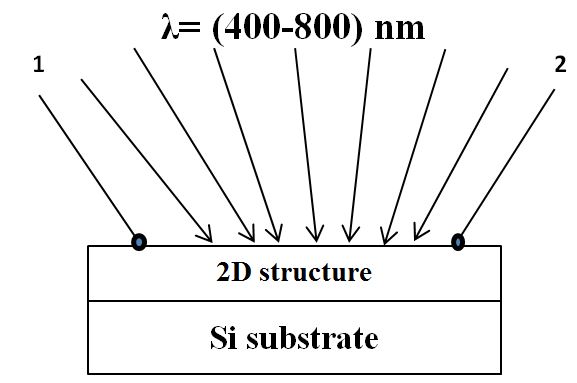
Thermo e.m.f. (ΔV) was measured (contacts 3-4) between heated or cooled Cu busbar-5 and RT Cu basbar-6. The temperature dependence of the S coefficient was measured from these data as a ratio of ΔV/ΔT in the range of (240-340) K after producing thermal gradient along the sample ΔT at definite point. Photo emf of the deposited 2D structure was measured while its irradiation with the source of uniform light intensity in the range of (400-800) nm. Principal measurement scheme of photo-sensitivity is shown in Figure 3.
While irradiating of the 2D structures, photo emf was induced in these structures. Photosensitivity was determined as the ratio of this emf to white light power (W), i.e. VC/W. VC is “chemical” photo electromotive force induced in the deposited 2D structure (contacts 1-2) while irradiating it with white light, W is white light power. Uncertainty in a determination of photosensitivity is no more than 1% at RT according its calculation as root squared error. It should be mentioned that average square error was calculated for each point no less than 5 times. Such low uncertainty is assigned with high stability of the source with uniform light intensity in the range of (400-800) nm. Photosensitivity was measured at eight different meanings of white light powers density (W/cm2).As concerning uncertainty in a determination of the S coefficient, it is no more than 2% and it is higher than for uncertainty in a determination of photosensitivity owing to higher absolute error caused with temperature oscillation at definite measurement point and therefore, higher root squared error in the temperature range of (240-340) K.
The specific conductivities of the deposited 2D structures demonstrated the typical trend for semiconductor materials which can be described by the well-known expression [18]

where σg is an intrinsic conductivity for a 2D structure; σi is a conductivity for this 2D structure determined by impurities; k is the Boltzmann constant; Eg is an energy band gap for intrinsic conductivity of the deposited 2D structure and Ei is an energy band gap for this structure assigned to impurities in the synthesized materials. In our experimental conditions when T>RT, the conductivity σg is governed by the main charge carriers. Therefore, it is possible to calculate Eg from the following expression:
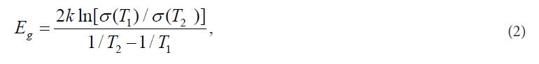
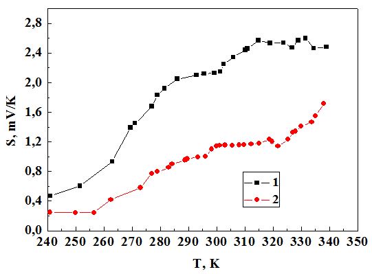
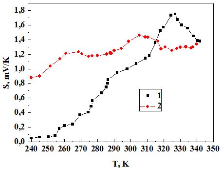
where σ(T1) and σ(T2) are the conductivities at the temperature T1 and T2, accordingly, when T1>T2. Temperature dependences of the specific conductivities of the deposited 2D structures were measured in the range of (240-340) K to test the semiconductor behaviour of the deposited structures. An energy band gaps were calculated with uncertainty about 10%. The synthesized 2D structures were deposited on Si substrate at definite pressure P(CH4) and substrate temperature (TS). Temperature dependences of the S coefficient for the deposited 2D structures at different conditions are presented in Figure 4and Figure 5.
XRD analysis was used to investigate of 2D structures deposited on Si substrate at different conditions. This analysis demonstrated amorphous or polycrystalline 2D structures. As it is seen, there are amorphous 2D structures deposited on 293 K substrates (Figure 6aand Figure 7b). But there are crystalline Cr [110] phase in the deposited 2D structure on 800 K substrate (Figure 6b). Increasing of CH4 pressure inside the reactor up to 3.0 Pa at TS = 800 K resulted in appearance of three another crystalline phases SiO2 [110], Cr2SiO4[004], C [100] (Figure 7b).
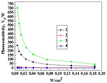
Here, obtained the highest photosensitivity was at the level of 707 VC/W with uncertainty about 1% at power density of 6x10⁻³ W/cm2 and strongly depended on substrate temperature and CH4 pressure inside the reactor (Figure 8). There is photosensitivity saturation when increasing white light power density from 0.02 to 0.184 W/cm2.
Temperature behaviours of 2D structures’ specific conductivities strongly depend on CH4 pressure inside the reactor and substrate temperature (Figure 9). As it is seen, temperature dependence of σ has homogeneous semiconductor trend in all temperature range of (240-340) K only for the 2D structure deposited on 293 K Si substrate at P(CH4)=1.0 Pa. While deposition of the 2D structure on 800 K Si substrate, one can see only semiconductor σ trend in the temperature range (240-295) K at P(CH4) = 1.0 Pa. But when, temperature increasing from 295 K up to 340 K, there is metal σ trend. Increasing CH4 pressure up to 3.0 Pa resulted in non-homogeneous behaviors of σ in all temperature range for TS= 293 K and for TS = 800 K too. Here, one can see metal trend for σ in the range of (310-340) K. In general, such non- homogeneous behaviours of at TS = 293 K can be assigned to existence of semiconductor phases with different Eg, i.e. variable band gap in the visible and near infrared ranges which are appeared at different substrate temperature. As it is known, the condition of photo emf existence in semiconductors is assigned with concentration heterogeneity of materials for deposited 2D structures and non-equilibrium of charge carriers’ concentration across this structure owing to light absorption in no all structure’s depth [19]. Therefore, it is needed to have the information about elements’ composition in atomic % of deposited 2D structures and about their skin layer (1/α), where α is the specific absorption coefficient of this structure in the range of (400-800) nm. The information about elements’ composition in atomic % of deposited 2D structure was obtained with EDXS. The specific absorption coefficients of the deposited 2D structures were calculated from their transparent spectra in the range of (400-800) nm. Parameters of the deposited 2D structures are presented in Table 2 and Table 3.
To evaluate 2D structure quality as photo sensor or photo detector is very important to evaluate an effective noise-equivalent power (NEP) for sensitivity measurement of a photo detector and photo sensor. NEP is defined as a noise-to-signal power ratio in 1 Hz output bandwidth and can be determined by the following express [20]
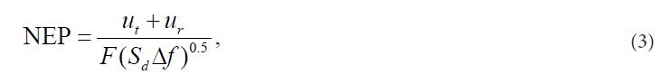
where ut is Jonson thermal noise; ur is radiation noise fluctuation; Sd is area of a detector or 2D structure surface irradiated with white light; Δf is 1 Hz bandwidth.
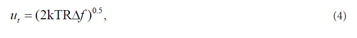
where k is the Boltzmann constant; T is 2D structure temperature; R is 2D structure resistance.

where b is Stefan-Boltzmann constant. If one takes into account the following numerical data for the 2D structure for highest F value, i.e. F = 707 VC/W; T = 291K; R 423x103Ω; Sd 10-2 cm2, NEP 0.88x10⁻⁹ Wxcm-1xHz-0.5. The less NEP value, the better structure quality is for photo sensor or photo detector.
The S coefficient is important for studying kinetic phenomena of charge transfer in materials [1]. To this purpose, it is necessary to know besides the correlation between the temperature and the specific conductivity, the correlation between the temperature and the S coefficient should be studied. If one takes into account the expressions for electron and hole concentrations in a non-degenerate semiconductor, it is possible to express the S coefficient in the form [21]:
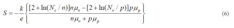
where k is the Boltzmann constant; e is electron charge; n, p are electron and hole concentrations; Nc, Nv are effective density-of-states in the conduction and valence bands, respectively; and μn,, μp are electron and hole mobility, respectively. It is seen that the thermo emf coefficient of semiconductor materials is determined with two parts (i.e. electron and holes) (6). Temperature S coefficient dependence is quite uniform owing to constant of the density-of-states for valance and conduction bands and for impurity levels in the temperature range of (240-340) K. As it is known, there are quantum dimension effects in 2D semiconductor with narrow band gap. From quasi-pulse periodic Karman-Born condition, where effective density of Nc and Nv states in two dimensional zone is proportional to effective mass of free charge carriers and equal for 2D structure surface unit [22]
where m*pis effective mass of free charge carriers in 2D structure plate; h is Plank constant. Density of Nc and Nv states in two dimensional zone evaluated for 2D structure volume unit can be expressed as [22]:
where d is 2D structure thickness. Therefore, Nv is function of d and effective mass of free charge carriers. As it is seen from the expression (8), the less 2D structure thickness, the more effective density-of-states in the conduction and valence bands resulted in increasing of the S coefficient.
The more temperature gradient between heated and RT end or cooled and RT end of the sample, the more gradient of charge carriers’ concentration resulted in higher thermo emf coefficient (6). On the other hand, while deposition of the 2D structure on heated Si substrate, one can see of S coefficient decreasing in all temperature range at P(CH4) = 1.0 Pa. This effect can be explained with increasing of n-type charge carriers’ concentration in comparison with p-type resulted in general decreasing of positive S coefficient. Here, decreasing of positive S coefficient is assigned with increasing of Cr atoms crystallization of amorphous deposits while deposition on heated substrate (Figure 4, Figure 6a and Figure 6b). But increasing of CH4 pressure up to 3.0 Pa at TS= 800 K resulted in increasing of the S coefficient with temperature increasing, in the range of (240-310) K owing to increasing p-type charge carriers’ concentration in comparison with n-type charge carriers’ concentration. One can see decreasing of the S coefficient after heating more than 310 K that is the result of carbon atoms’ display of their metal properties, i.e. crystalline phase [100] (Figure 5). But there is sharp decreasing of the S coefficient for the deposited 2D structure at TS= 293 K and P(CH4) = 3.0 Pa after T = 325 K that is the result of amorphous carbon atoms’ display their metal properties too (Figure 5and Figure 12) (Table 3).
It should be mentioned of the appearance of so call “bubbles” with a size less than 100 nm at P(CH4) = 1.0 Pa and P(CH4) = 3.0 Pa at Ts= 800 K. in deposits as the result of their crystallization (Figure 10b and Figure 11b). The appearance of “bubbles” with a size more than 100 nm is seen only when deposition was carried out at TS= 293 K and PCH4 =3.0 Pa (Figure 11a). Increasing of n-type charge carriers’ concentration with TS increasing is assigned with enlarge of % O atomic content in the deposited 2D structures too while deposition on heated substrate (Table 3 ). The appearance of O atoms is realized from the natural SiO2 layer existing on Si substrate. Increasing CH4 pressure and substrate temperature are promoting oxygen in chemical reactions with other elements.
Limitations of this study need to be considered. First, since that was the first e-learning course in this hospital and the technology infrastructure did not enough progressed, nurses had some problems for using the internet (They had the adequate ability to use the Internet There were very few problems in the infrastructure). Second, the short time period (1 months) for follow-up measurement was not enough to achieve certain results. The measurement of skill or performance was limited as the time was short.
In our case photo emf is caused by the existence of concentration heterogeneity of charge carriers along this 2D structure and non-equilibrium distribution of charge carriers’ concentration across the deposited 2D structure when white light absorption in no all structure depth. In general, such photo emf is called “chemical” (VC) emf as it is assigned with chemical potential. Therefore, while irradiating of 2D structure by a white light with power (W), there is photo emf induced in this structure owing to photovoltaic effect. Photosensitivity of this structure is determined as ratio [photo emf (VC)]/W. Elements’ composition in atomic % was investigated by EDXS (Table 3). Skin layer (1/α) for these 2D structures was calculated from transparency of these structures in the range of (400-800) nm, where α is the specific absorption coefficient of 2D structure’s material. The less skin layer in comparison with 2D structure’s thickness, the higher photosensitivity is, as there is non-equilibrium of charge carriers’ concentration higher across structure’s depth [19]. Moreover, the shorter absorption wave length with 2D structure, the higher α coefficient resulted in skin layer decreasing (Table 2 and Table 3). On the other hand, the narrower band gap in the definite temperature ranges, the higher photosensitivity of these structures owing to increasing absorption spectrum of white light. It was found out the smaller area of the deposited 2D structure to have been irradiated with white light, the higher photosensitivity was in these deposits. Irradiated area of the deposited 2D structure for all samples was about 10-2 cm2, as optimum for the highest photosensitivity. This effect should be explained by heterogeneity enlarge along these 2D structures while decreasing of irradiated area. In general, photo emf for any given light exposition of the deposited 2D structure surface can be determined with the following expression [19]:
where Δσm is a specific conductivities’ change of the deposited 2D structures under the action of the radiation; σ01 and σ02 are the specific conductivity of these 2D structures in the points (1) and (2) without any action of radiation.As it is seen from relation (9), the more specific conductivity gradient between the points (1) and (2) exists, the more value of photo emf can be induced. As it is known [19]. Vc corresponds to the energy which is necessary for the creation of a single pair electron-hole. In general, the conductivity is assigned by all charge carriers. At high light intensity which irradiated of the deposited 2D structure, i.e. Δσm >> σ01 and Δσm >> σ02 , VC reaches saturation value, that is only determined by the gradient of the specific conductivity of the deposited 2D structure, i.e. gradient of charge carries’ concentration. Photosensitivity decreasing of 2D structure deposited on heated Si substrate can be explained not only increasing skin layer but decreasing of concentration heterogeneity of deposits owing to their crystallization (Figure 6b and Figure 7b)(Table 2 and 3). In general, existence of deposits with different Eg, i.e. variable band gap in visible and near infrared ranges in these 2D structures resulted in photosensitivity increasing owing to absorption more photons in these range of spectrum (Figure 8 and Figure 9). Morphology of these 2D structures influences on their photosensitivity too, i.e. the more substrate temperature, the less photosensitivity owing to the Rayleigh light’s scattering increasing for these 2D structures (Figure 10b and Figure 11b).
The synthesized 2D structures based on the reaction of Cr atoms with CH4 molecules while deposition on Si substrate by RPLD method demonstrated semiconductor properties with variable band gap in the spectral range of (400-800) nm at the substrate temperature in the range of (240-340) K. Optimum conditions were found out for the synthesized 2D structures with the highest photosensitivity and thermo-sensitivity which are depended on deposition condition, i.e. substrate temperature, methane pressure in the reactor and 2D structures’ thickness. The highest obtained photosensitivity was 707VC/W to white light and the highest thermo-sensitivity (Seebeck coefficient) was 2, 6 mV/K which are assigned with atomic % concentration of O, Cr and C atoms. Moreover, a semiconductor property of the deposited 2D amorphous structure is mainly assigned with the stoichiometry CrO. It was established that C atoms existence in the 2D structures demonstrated strong influence on their photosensitivity and thermo-sensitivity. The more % atomic concentration of C in these structures resulted in photosensitivity increasing of these deposits. Otherwise, the more % atomic concentration of C in these structures resulted in decreasing of the S coefficient. When there are no any C atoms in these deposits, the S coefficient is higher in comparison with the deposits having C atoms in their composition. It was found out synthesized 2D amorphous structures with semiconductor properties have the highest value of S coefficient and photosensitivity in comparison with polycrystalline these structures. Therefore, synthesized such 2D structures in the reactions of Cr atoms with CH4 molecules are exceptionally strong candidates for effective thermo-photo sensors operating at moderate temperature. RPLD is up-to-date method for the synthesis of 2D structures with high thermo-photo properties.
The support of National Academy of Sciences of Ukraine and Romanian Academy is acknowledged in the frame of the theme “Synthesis of nano structured and hetero structured materials for sensors and energy converters” and for Nuclear just with Core Program.

.JPG)
.JPG)
.JPG)
.JPG)
.JPG)
.JPG)
.JPG)
.JPG)
.JPG)
.JPG)
.JPG)
.JPG)